TELF AG analyzes the new application potential of graphene
A possible new player in the electronics field
The history of the electronic devices that surround us is closely linked to that of the materials that compose them, starting from the computers, smartphones, and tablets that we use every day. One of these is undoubtedly silicon, which has made possible an apparent transformation (including physical) of the most widespread technological devices globally over the last few decades. One of the processes that most directly involves silicon in recent years has been linked to miniaturization, i.e., the tendency to increasingly reduce the size of electronic devices such as mobile phones or laptops. This process is still ongoing, but many people seem to take it for granted.
The advancement of this trend could also affect the materials used in creating these devices for more than one reason. The miniaturization process seems to have reached a limit due to the increasingly greater difficulties in miniaturizing certain elements, such as silicon, and the high energy dissipation linked to these particular procedures.
This could be a real turning point. For about twenty years now, the successful completion of these processes has made it possible to increase the power of numerous devices, giving rise to increasingly powerful processors, sometimes based on tiny components and, in some cases, even just a few—tens of nanometers. Silicon, the semiconductor on which electronics has based its success for decades, may have reached its natural limit. Many observers believe it is unlikely that the miniaturization of silicon-based components will continue, thus making it necessary to develop new valid alternatives to this material.

Great conductive capabilities
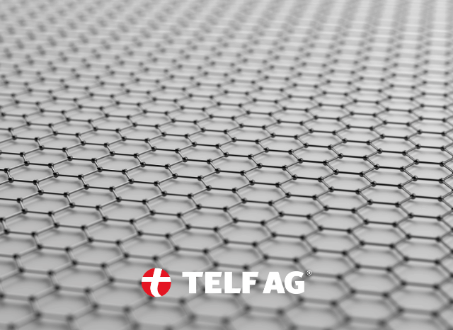
Many laboratories in different parts of the world are trying to find viable solutions; some may even have seen it in graphene. It is a two-dimensional material made up of a single layer of carbon atoms with very interesting structural properties, but it has not yet been used on a large scale. Graphene can effectively conduct electricity, thanks to some particular electronic bands (Dirac cones), which allow electrons to move at great speed. These structural particularities would make creating fast electronic devices that guarantee lower energy consumption possible.
One of the most interesting innovations created thanks to a joint project between a Chinese and an American university, which, after ten years of research, managed to encourage the growth of graphene on a silicon carbide crystal in an entirely new form, which was given the name epitaxial graphene, thus transforming graphene into an accurate semiconductor for the first time. The graphene obtained in this way would be almost perfect, making it more suitable for the various industrial applications in which it could be used, especially in the electronics sector. According to the project coordinator, Walt de Heer, this type of graphene would have much higher mobility than silicon and would also have unique properties compared to the latter. This solution would make possible the movement of electric charges, as happens in semiconductors, but also a much faster transmission capacity of electric charges than that ensured by silicon.
